
GRID
The PCB Editor is a grid-based design environment – design objects are placed on what is referred to as the placement, or snap grid. As well as the placement grid, the software includes a number of additional snap features, designed to help you accurately position and align design objects.
UNDERSTANDING THE GRID
In the schematic editor we never even looked at the grid, but in the board editor it becomes much more important. The grid should be visible in the board editor. You can adjust the granularity of the grid, by clicking on the GRID icon —  . A 0.05″ grid, and 0.005″ alternate grid is a good size for this kind of board.
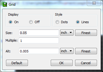
EAGLE forces your parts, traces, and other objects to “snap” to the grid defined in the Size box. If you need finer control, hold down ALT on your keyboard to access the alternate grid, which is defined in the Alt box.
Let me paint a few pictures for you:

Notice how in this image I have set the grid size to 0.8mm which matches the IC and I can get the capacitor to align perfectly to the pin? Well, now the SOIC-16 is also aligned to the same grid but the problem is that component’s pin pitch is 1.27mm which means the capacitor won’t align to the pin perfectly and looks fairly ugly now.
Now take a look at this:
